“At present, the status of solar photovoltaic companies is miserable and catastrophic. Affected by this, the electronic gas industry entered early winter, prices fell sharply, sales were almost stagnant, and the debts were difficult to recover. Many companies had already shut down the production line. The year 2012 will be the culmination of the past several years for China’s electronic gas.†At the 22nd Member Representative Conference of the China Industrial Gas Industry Association held in Yanji City, Jilin Province on October 18-23, and the 2012 annual meeting, mentioning electronics The current status of the gas industry market, Sun Funan, chief engineer of the Sinochem Bright Chemical Research & Design Institute, is worried. Sun Funan told reporters: “The photovoltaic, LED, and IC industries are the main application areas for electronic gas. Not only are there large quantities of demand, but also many types, and the PV industry’s annual demand for silicon tetrahydride and high purity ammonia is in the thousands of tons. Compared with previous years, the three major downstream industries of electronic gas have become completely different this year." He explained that in the last 3 to 5 years, under the encouragement and support policies of local governments, the domestic photovoltaic industry has seen a spurt expansion and the production capacity has been excessively surplus. This time, the United States has implemented "double opposition" to China's photovoltaic products, involving 75 domestic companies, and the EU is likely to take the opportunity to follow suit. At the same time, photovoltaic companies that have already closed down in the United States have also sought compensation from Chinese companies through judicial procedures. 90% of China's solar energy products are sold abroad, of which 80% are in the European Union. Anti-dumping cases in the European Union and the United States will cause the Chinese photovoltaic industry to lose about 130 billion yuan in the market. In 2012, many large-scale PV companies reduced their production or semi-discontinued production. The domestic PV giants listed in the United States faced delisting or even bankruptcy. Compared with photovoltaic solar energy, the LED is slightly better. However, China's LED industry is undergoing a major leap forward, and overcapacity is now emerging. According to incomplete statistics, by September 2012, LED lighting companies in Zhejiang had rapidly increased from the initial 16 to about 180, and this number is still increasing. Sun Funan lamented: "Unfortunately, most of the lighting companies that have entered the LED are producing low-end products. The high-end core technology and product markets are still controlled by foreign countries. If we do not adjust the overall strategy as soon as possible, blindly pursue the increase in volume, or Will cause our country LED industry to become the next photovoltaic. In the first few months, the domestic LED market has been difficult to sell, sales dropped. "In addition, the Chinese IC industry is taking the road of generation processing. Due to the deteriorating background, the current production has dropped sharply, which is already less than 50% of previous years, and this trend is still intensifying. Sun Funan concluded that once the funds are broken, there will be a large number of photovoltaic, LED and IC companies going bankrupt. This has led to a number of e-gas production and distribution companies that have closed down, and those that have barely maintained production are worried about poor product sales, while those who sell products have to worry about difficulties in recovering arrears, and are caught in a difficult situation. Don't sell everything." The pressure faced by the electronic gas industry is more than that. Sun Funan told reporters: "After the last three years of development, China has successfully ended the history of domestically produced electronic gas that could not be mass-produced and stable. High purity ammonia, hydrogen chloride, carbon tetrafluoride, nitrogen trifluoride, sulfur hexafluoride The domestic electronic gas represented by the company is well represented in the fields of photovoltaics, LED, and IC (8 inches and above), and the new high-purity silane technology has been able to form a stable and safe production of thousands of tons after years of research and development. Capacity, domestic silane products not only gain market application, but also have extremely competitive prices, only 0.4-0.6 yuan/g, while import prices have reached 3 yuan/g. Due to the leap-forward development of domestic gas in terms of quality and output, international gas The company changed its development strategy in China and began to accelerate the construction of high-tech electronic gas production lines in China." Take this year's hot high-purity ammonia as an example. Overseas companies such as AP, Air Liquide, Linde, and Sumitomo Japan have begun to build ammonia purification lines near LED users, and Asian ammonia production companies such as Korea PSG are planning to change their sales methods. At present, China's foreign-funded high-purity ammonia production capacity alone exceeds 13,000 tons/year. If we add domestically produced high-purity ammonia production capacity, our country's high-purity ammonia supply has exceeded supply. The market price of high-purity ammonia has dropped sharply, and has dropped from more than 100 yuan per kilogram in previous years to several tens of yuan, and it is still falling, showing the fierce competition. However, some electronic gas products represented by high-purity nitrous oxide are still in short supply. Unfortunately, domestic companies do not possess core technologies. Sun Funan stated: “High input, high returns, and high risks are the characteristics of high-tech products, and the high-purity gases that are matched with them have the same characteristics. The electronic gas industry is in a predicament, although the US PV dual-reaction case is an important driver, but the key It is also that the industry is still at the level of low-end product duplication." Sun Funan stated that mastering core technologies is the key to winning competition. After rapid development in previous years, some companies have realized capital accumulation. It is hoped that such enterprises can increase the research and development of new products and new technologies and strengthen brand cultivation. The entire industry will strive to achieve effective integration of capital, technology, market and region as soon as possible. Fill the electricity for the next round of competition, and strive to turn the once-brilliant end point of electronic gas into the starting point of the industry's rebirth. PCB Stencil
PCB Stencil, SMT Stencil, SMD Stencil, Laser Stencil, What is it?
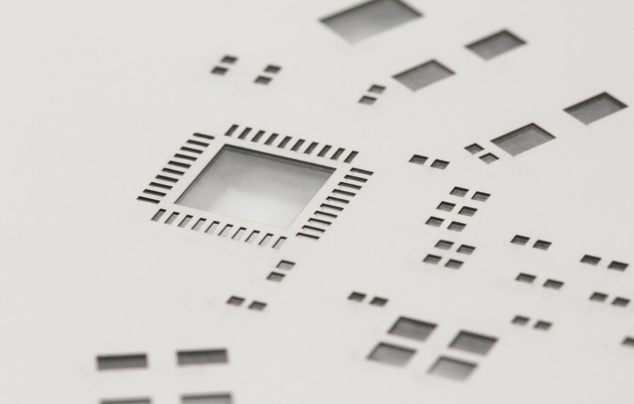
The openings are etched into the metal using acid. Usually this kind of stencil offers better protection on material temper and hardness.
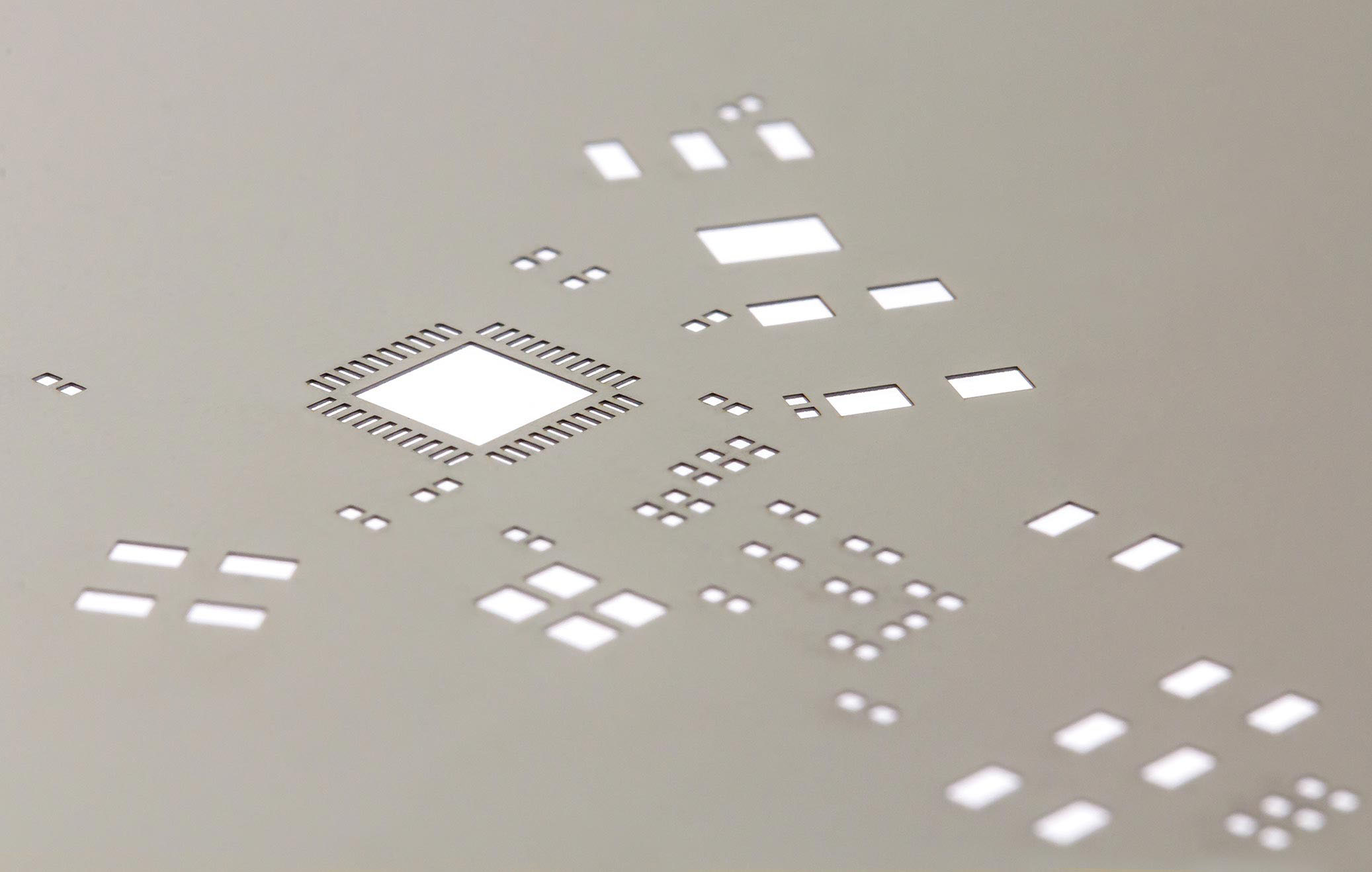
When prototyping dictates fast action with minimal cost, our prototype stencils are the best solution. Prototype Stencils gives you a quality stencil and framework so you can handle assembly from the convenience of your own desk.
Includes Prototype Stencil, one board holder, leaded or lead-free solder paste (must specify), temperature marker, squeegee, ESK-safe gloves and alcohol wipe.
Handy and convenient for low quantity prototype assembly using the Prototype Stencils. Re-usable, includes vacuum bulb and vacuum clips with diameters of 3/8", 1/4", and 1/8".
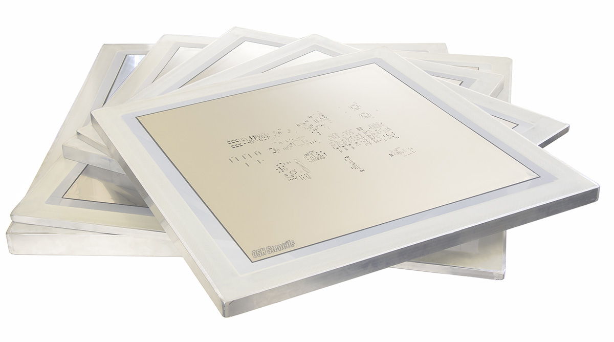
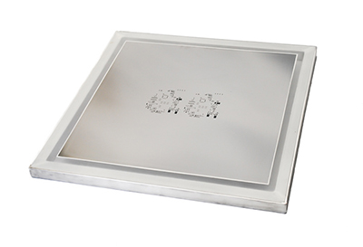
Framed stencils are laser-cut stencils designed for high volume screen-printing. With a framed stencil, your stencil is securely mounted to either a cast or extruded aluminum stencil frame a stencil frame using a mesh border, allowing for complete control.
Framed PCB Stencil Area
Maximum Squeegee Area
300mm*400mm (11.81inch*15.75inch)
120mm*220mm (4.72inch*8.66inch)
370mm*470mm (14.57inch*18.5inch)
200mm*300mm (7.87inch*11.81inch)
400mm*600mm (15.75inch*23.62inch)
220mm*400mm (8.66inch*15.75inch)
400mm*700mm (15.75inch*27.56inch)
220mm*500mm (8.66inch*19.69inch)
400mm*800mm (15.75inch*31.5inch)
220mm*600mm (8.66inch*23.62inch)
400mm*900mm (15.75inch*35.43inch)
220mm*700mm (8.66inch*27.56inch)
400mm*1000mm (15.75inch*39.37inch)
220mm*800mm (8.66inch*31.5inch)
400mm*1200mm (15.75inch*47.24inch)
220mm*1000mm (8.66inch*39.37inch)
400mm*1400mm (15.75inch*55.12inch)
220mm*1200mm (8.66inch*47.24inch)
420mm*520mm (16.54inch*20.47inch)
240mm*340mm (9.45inch*13.39inch)
450mm*550mm (17.72inch*21.65inch)
270mm*370mm (10.63inch*14.57inch)
500mm*800mm (19.69inch*31.5inch)
320mm*600mm (12.6inch*23.62inch)
500mm*1200mm (19.69inch*47.24inch)
320mm*1000mm (12.6inch*39.37inch)
550mm*650mm (21.65inch*25.59inch)
340mm*440mm (13.39inch*17.32inch)
584mm*584mm (23inch*23inch)
380mm*380mm (15inch*15inch)
736mm*736mm (29inch*29inch)
480mm*480mm (19inch*19inch)
Foil or Plate Only stencils are designed to work within interchangeable plate or "universal" systems. Also referred to as "reusable", these stencils do not need to be permanently glued into a frame.
For times when you need precise control for smaller production runs, our Foil or Plate Only stencils are ideal. These frameless stencils allow you to hand print with precision just the amount you need and can be stored conveniently.
Electroformed SMT stencils are nickel-based, electroform foils permanently mounted in a stencil frame using a mesh border to tightly stretch the stencil foil taut in the frame. Electroformed stencils offer the best paste release characteristics available and are frequently used for fine pitch (20 mil to 12 mil pitch) SMT applications on printed circuit boards. They are also used for µBGA's, Flip Chip, and Wafer Bumping (12 mil to 6 mil pitch).
PCB designers have to focus on internal size of stencil, they don't need to care about its overall size since it is generally determined by the parameters of printer in your contract assembler workshop.
PCB Stencil,SMT Stencil,SMD Stencil,Laser Stencil JingHongYi PCB (HK) Co., Limited , https://www.pcbjhy.com
PCB SMT Stencil,the unique goal is to move solder paste to the bare printed circuit board.
Apart from all types of Printed Circuit Boards (PCBs) such as Prototype PCB, Aluminum PCB , HDI PCB , Flexible PCB , Rigid Flex PCB, Thick Copper PCB, High TG PCB , JHYPCB also manufactures solder paste stencils to meet Surface Mount Technology (SMT) requirements.
PCB Stencils, also called SMT stencils, SMD stencil, play a key role in transferring accurate amount of solder paste to correct positions on bare circuit boards ready for assembly. In other words, stencils can fast and efficiently ensure the most accurate solder paste amount and optimal electrical connection. With solder stencils, it is possible to use metal squeegee blades to apply solder paste easily over the openings on PCBs and make stencil to be well aligned with the surface of the advanced circuit board.
All of our SMT Stencils are 100% laser-cut type 304 full-hard stainless steel, ensuring the finest quality finish on the market today. We use a .001" laser beam with 98% overlap creating an extremely smooth hole that provides the best paste release. Most stencil fabricators use a .003" laser leaving mouse bites on the aperture edge. You can choose a PCB Prototype stencil, a frameless foil stencil, or a rigid permanently mounted stencil. Both the frameless and framed stencils come in various sizes to accommodate your printer and stencil requirements.
PCB Stencil Types Available:
1. Laser-cut stencils
The openings are lasered on 100% stainless steel. Generally speaking, this kind of stencil can be produced with high quality and a high degree of precision within a short time.
2. Chemical-etch stencil
3. Prototype PCB Stencil (Low-volume manual printing. Ideal for prototypes)
Prototype SMT Stencil Features:
Prototype
SMT Stencil Specs:
Technology
100% laser cut
Material Used
Stainless Steel
Stencil
Thickness
0.06 ~ 0.3 mm
Minimum Cut
Width
0.05 mm
Maximum Size
736 X736 mm
Aperture
Tolerance
within 0.007mm
Allow for
Fiducial Data
Yes
Delivery
1 ~2 Day
4. NEW Prototype PCB Stencil Kit (with leaded or lead/free solderpaste)
5. NEW Pick and Place Tool
6. Framed SMT Stencils (Also called "Glue-in" or Mounted Stencils)
Framed SMT Stencil Features:
Framed
SMT Stencil Specs:
Technology
100% laser cut
Material Used
Stainless Steel
Frame Types
Cast, Space Saver
Stencil
Thickness
0.06 ~ 0.3 mm
Minimum Cut
Width
0.05 mm
Maximum Size
736 X736 mm
Aperture
Tolerance
within 0.007mm
Allow for
Fiducial Data
Yes
Allow for
Panelized Data
Yes
Delivery
1 ~2 Day
Framed PCB Stencil Specification
7. Frameless SMT Stencil - Foil/Plate Only (for universal frames)
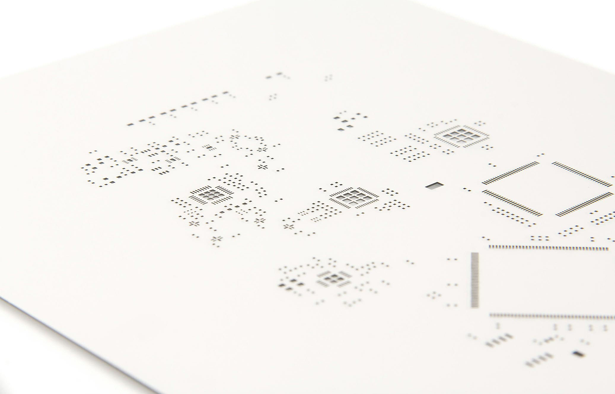
Frameless SMT Stencils also referred to as foils are laser cut solder paste stencils designed to work with stencil tensioning systems known as reusable stencil frames. This type of stencil does not need to be permanently glued in a frame. Frameless stencils are significantly less expensive than framed stencils and provide money-saving storage while still delivering superior quality and performance.
Frameless SMT Stencil Features:
Frameless
SMT Stencil Specs:
Technology
100% laser cut
Material Used
Stainless Steel
Stencil
Thickness
0.06 ~ 0.3 mm
Minimum Cut
Width
0.05 mm
Maximum Size
280 X 380 mm
Allow for
Fiducial Data
Yes
Allow for
Panelized Data
Yes
Delivery
1 ~2 Day
8. Frameless SMT Stencil - Foil/Plate Only (for hand printing)
9. Electroformed SMT Stencils
Electroformed SMT Stencil Features:
Electroformed
SMT Stencil Specs:
Technology
Electroforming
Material Used
Nickel
Suitable
Applications
All Component Pitches
Aperture
Tolerance
within 0.007mm
Stencil Thickness
0.06 ~ 0.3 mm
0.06mm.0.08mm.0.1mm.0.12mm.0.13mm.0.15mm.0.18mm.0.2mm.0.3mm
Positional
Accuracy
± 0.008mm
Delivery
1 ~2 Day
What's the difference between a framed stencil and a frameless stencil?
A framed PCB stencil will have a 0.5" to 1.5" thick metal frame around it, similar to a picture frame. Framed stencils are often used by contract manufacturers, assembly and board houses, and large scale production facilities and are commonly placed in a manual or automated stencil printing machine. Frameless stencils are a thin sheet of material cut with a small border around your design. For example pictures on these products, please visit our Gallery.
What's the difference between Polyimide and Stainless Steel?
All stencils are made with high quality Polyimide and Stainless Steel. We use only the industry leading Stainless Steel, designed specifically for stencils. These materials are ideal for prototype or Multilayer PCB.
Stainless Steel: 0.0007" Laser spot size, 0.001" minimum aperature size.
Polyimide Film: 0.003" Laser spot size, 0.005" minimum aperature size.
Polyimide has a lower precision rate due to the way it is processed and its ability to withstand heat during the cutting process. Minor variances will occur when the material reacts to the laser. Paste release is great, but this material should be limited to a small number of uses and with components 0402 or bigger.
The minimum aperature size for Polyimide is 0.005" vs 0.001" for Stainless Steel. Polyimide also has a natural curl in the material caused by the way the film is manufacturered, this is outside of our control. Stainless Steel provides the ultimate in precision and quality, with a 0.0007" spot size, and exceptional paste release with a truly flat surface. If you want the absolute best reflow experience, there is no comparison, Stainless Steel is the superior material.
Analysis and Treatment of Common Problems in PCB SMT stencil
Insufficient solder paste may cause poor bonds and contact between components and the board. The common causes of insufficient solder paste are poor gasketing, clogged stencil apertures, insufficient solder paste bead size, paste/stencil being used beyond recommended life span, stencil not wiped clean, or low squeegee pressure.
The main causes of smudging/bridging are excessive squeegee pressure, inadequate stencil wiping, poor contact between the board and stencil, high temperature or humidity, or low solder paste viscosity.
A typical misalignment print is usually caused by the vision system not spotting fiducials, PWB or stencil stretch, poor contact between the board and the stencil, or weak board support.
A PCB board not fixed properly during solder paste printing gives poor results and increases soldering related issues. Normally, solder paste printing equipment can handle warpage of 1.0 to 3.0 mm but beyond this limit needs some special jigs or fixtures to hold the PCB. It may be difficult to tackle thick and small boards compared to thin and bigger size boards.
How to Determine Stencil Size?
Stencil size is composed by two parts: internal size and overall size. Internal size is the size compatible with that of PCB ready to be assembled while overall size refers to the size compatible with printer parameter limit. As long as both sizes are accurately designed, stencil will be able to make full use of its functions.
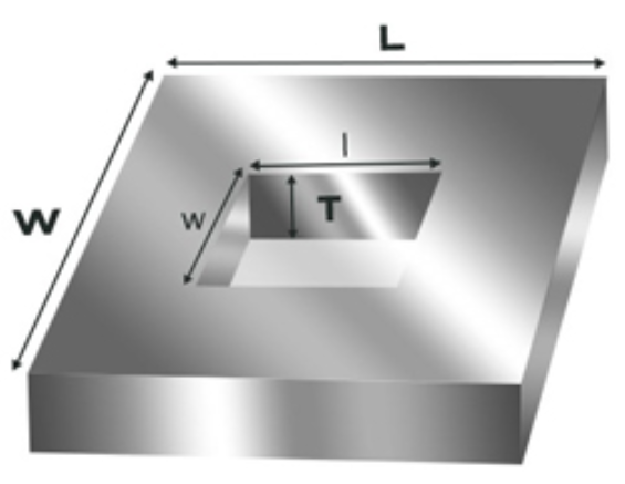
Internal size of stencil can be figured out conforming to the following rule:
For example, if one circuit board size is 50*50mm, then the size of its framed stencil should be around 150*150mm and the size of its frameless stencil should be around 250*250 mm.
It's easy to remember and operate so it worked for manual solder paste printing in SMT assembly prior to the advent of automatic printer. It can be said that different PCB sizes lead to generations of different internal sizes of stencil.
When it comes to automatic solder paste printer, however, it's relatively solid. Overall size of stencil has to be determined by parameter limit of the equipment, that is, printer, because stencil has to work within the range of printer with a frame. Different printers feature different parameter regulations. As far as PCBCart is concerned, the stencil size compatible with our printer can be either 650mm*650mm or 736mm*736mm.
How to Use PCB SMT Stencils?